Design and Timing in the Real World Closure is all about implementing chips, optimizing them, and getting designs ready for signoff for high-performance VLSI systems.
Level
Advanced
Duration
8 Weeks
Placement Client


.png)












.png)


About Physical Design & Timing Closure
Rated #1 Recognized as the No.1 Institute for Physical Design & Timing Closure Design Online Training Course. This program teaches you everything you need to know about the ASIC back-end design flow. It includes synthesis, floorplanning, placement, clock tree synthesis (CTS), routing, and optimization after routing. The course focuses on getting timing closure by dealing with constraints, fixing signal integrity, and making trade-offs between power and performance. By the end, students will have used industry-standard tools and be ready for tape-out projects.
Training Plan
About trainer
Working professional who is carrying more then 10 years of industry experience.
Decks & Updated Content
Access to updated presentation decks shared during live training sessions.
e-Book
E-book provided by TechPratham. All rights reserved.
Assignments & MCQs
Module-wise assignments and MCQs provided for practice.
Video Recording
Daily Session would be recorded and shared to the candidate.
Projects
Live projects will be provided for hands-on practice.
Resume Building
Expert-guided resume building with industry-focused content support.
Interview Preparation
Comprehensive interview preparation with real-time scenario practice.
Physical Design & Timing Closure Course Curriculum
Introduction to Physical Design
Overview of physical design flow and its role in ASIC implementation.
Floorplanning & Power Planning
Chip floorplanning and power grid design.
Placement & Optimization
Standard cell placement and congestion management.
Clock Tree Synthesis (CTS)
Clock distribution and skew management.
Routing & Physical Optimization
Signal routing and post-route optimization.
Static Timing Analysis (STA)
Timing analysis for meeting performance goals.
VLSI Embedded Systems And Chip Design Courses
No related courses found
Additional Program Highlights


Upcoming Batches
Can't find a batch you were looking for?
Who Should Take Physical Design & Timing Closure
IT Professionals
Non-IT Career Switchers
Fresh Graduates
Working Professionals
Ops/Administrators/HR
Developers
BA/QA Engineers
Cloud / Infra
IT Professionals
Non-IT Career Switchers
Fresh Graduates
Job Roles For Physical Design & Timing Closure
Key Projects
Physical Design & Timing Closure
ASIC Block-Level Physical Design
Implement a block-level design from synthesis to routing. Optimize timing, area, and power while ensuring clean DRC and LVS for signoff.
Full-Chip Floorplanning & CTS Project
Develop a full-chip floorplan including power grid and I/O placement. Perform CTS to minimize skew/latency and validate with STA.
Timing Closure for Multi-Corner Design
Work on a design targeting multi-corner timing closure. Apply ECO fixes, optimize for PVT variations, and prepare the design for tape-out.
Placement Process
Live Class with Industry Use Cases
- Interactive learning
- Real-world examples
- Expert guidance
- Doubt resolution
Daily Assignment & Weekly Assessments
- Hands-on practice
- Concept reinforcement
- Weekly evaluation
- Timely feedback
Project Testing & Deployment
- Project development
- Testing practice
- Deployment exposure
- Portfolio creation
Interview Preparation (Mock, PD, Alumni Session)
- Mock interviews
- Personal development
- Alumni guidance
- Confidence building
Resume Building
- Resume crafting
- Industry-focused format
- Skills highlighting
- Professional presentation
Placement
- Job assistance
- Interview support
- Career guidance
- Opportunity access

Knowledge Center
Recently Placed Candidates
We’re Hiring
News Highlights
Our Success Mantra
 Commitment
- Ensuring quality training every day
 Fulfillment
- Meeting learning goals with confidence
 Accomplishment
- Students achieving industry-ready expertise
Our Learner Voice
Beyond Courses:
Additional Support We Provide
24/7 Support
LinkedIn Profile
Resume Writing
Alumni Sessions
Interview Preparation
Live Projects
What Makes TechPratham Training Different?
What skills will I gain from this course?
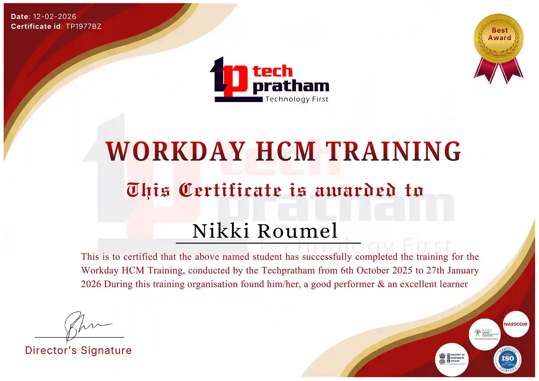
Industry-Recognized Certification
India
India
Noida Office
C-2, Sector-1, Noida, Uttar Pradesh - 201301
India
Hyderabad Office
LVS Arcade, 6th Floor, Hitech City, Hyderabad


 View on Google Maps