



Rated #1 Recognized as the No.1 Institute for Semiconductor Fabrication Technology Online Training Course. We teach both hands-on and theoretical methods for wafer processing, lithography, doping, thin-film deposition, and etching. The course covers the whole process of making semiconductor devices, with a focus on CMOS, VLSI, and nanoelectronics. Students will learn about real-world fabrication workflows, process integration, and ways to improve yield. This program is great for people who want to work in semiconductor design and manufacturing, whether they are students or professionals.
VLSI Embedded Systems And Chip Design
Semiconductor Fabrication Technology
Semiconductor Fabrication Technology Online Training provides in-depth knowledge of IC manufacturing processes, cleanroom practices, and nanotechnology techniques. It equips learners with skills to understand and design semiconductor devices at the fabrication level.
5/5(4,890 Reviews)
Level
Advanced
Duration
8 weeks
Placement Client

.png&w=3840&q=75)









About Semiconductor Fabrication Technology
Training Plan
01

About trainer
Working professional who is carrying more than 10 years of industry experience.
02

Decks & Updated Content
Access to updated presentation decks shared during live training sessions.
03

e-Book
E-book provided by TechPratham. All rights reserved.
04

Assignments & MCQs
Module-wise assignments and MCQs provided for practice.
05

Video Recording
Daily Session would be recorded and shared to the candidate.
06

Projects
Live projects will be provided for hands-on practice.
07

Resume Building
Expert-guided resume building with industry-focused content support.
08

Interview Preparation
Comprehensive interview preparation with real-time scenario practice.
<p>Semiconductor Fabrication Technology</p> Course Curriculum
VLSI Embedded Systems And Chip Design Courses
Additional Program Highlights
Comprehensive study materials and resources
HD
Professional resume building session
HD
Master your interview skills
HD
Real-world project demonstrations
HD
Upcoming Batches
Can't find a batch you were looking for?
Who Should Take <p>Semiconductor Fabrication Technology</p>
IT Professionals
Non-IT Career Switchers
Fresh Graduates
Working Professionals
Ops/Administrators/HR
Developers
BA/QA Engineers
Cloud / Infra
IT Professionals
Non-IT Career Switchers
Fresh Graduates
Key Projects
<p>Semiconductor Fabrication Technology</p>

CMOS Fabrication Flow Simulation
Use semiconductor CAD tools to simulate the entire CMOS fabrication process, which includes steps like lithography, doping, and deposition.

Lithography Mask Design
Create a mask for semiconductor patterning and check its resolution limits with different lithography methods.

Process Variation Impact Study
Examine how changes in the process (doping levels, etching depth, deposition thickness) affect the performance and yield of the device.
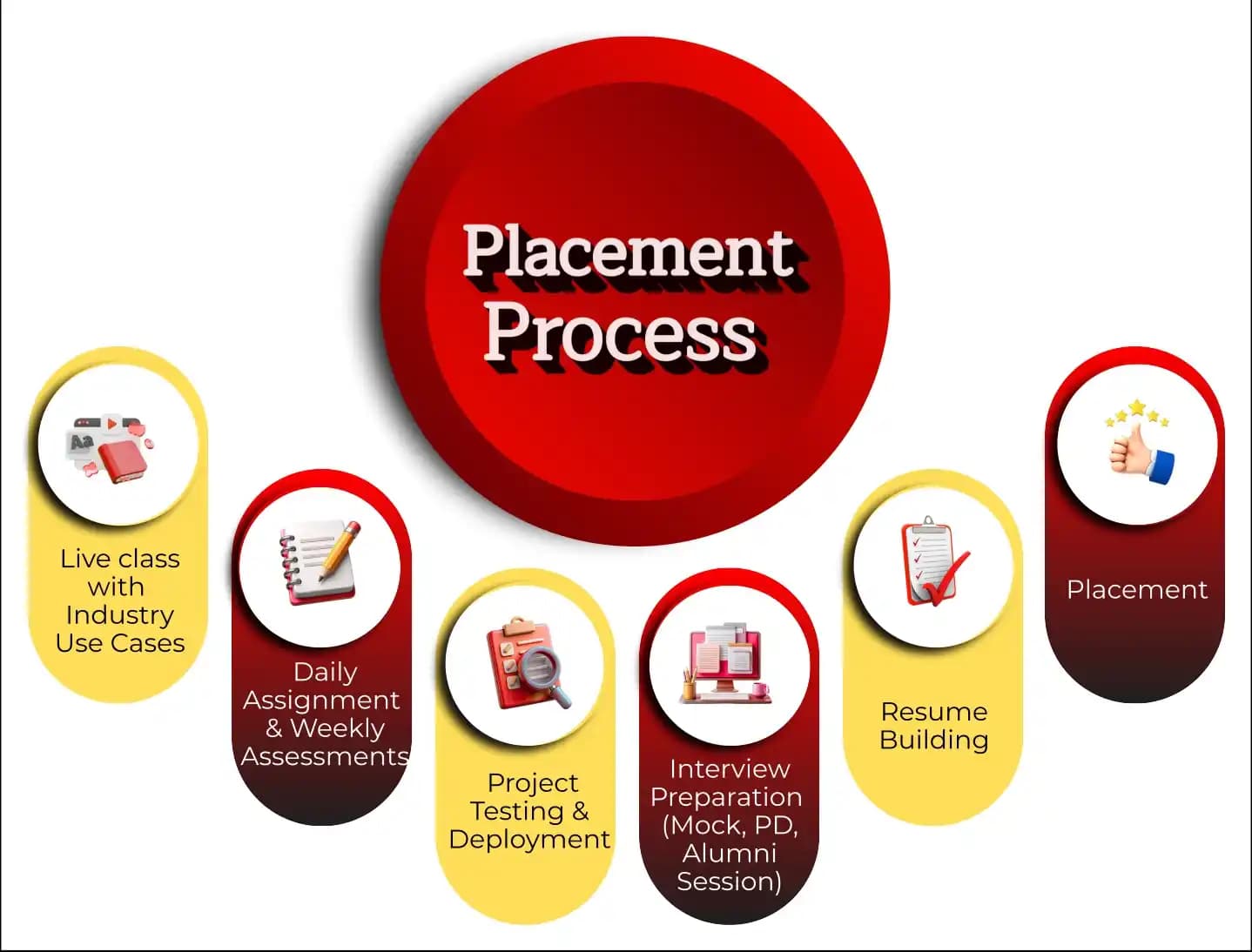
Placement Process

Live Class with Industry Use Cases
- Interactive learning
- Real-world examples
- Expert guidance
- Doubt resolution

Daily Assignment & Weekly Assessments
- Hands-on practice
- Concept reinforcement
- Weekly evaluation
- Timely feedback

Project Testing & Deployment
- Project development
- Testing practice
- Deployment exposure
- Portfolio creation

Interview Preparation (Mock, PD, Alumni Session)
- Mock interviews
- Personal development
- Alumni guidance
- Confidence building

Resume Building
- Resume crafting
- Industry-focused format
- Skills highlighting
- Professional presentation

Placement
- Job assistance
- Interview support
- Career guidance
- Opportunity access
Latest Hiring
No hiring posts
Recently Placed Candidates
No placements available
Latest Hiring
No hiring posts
Our Success Mantra
 Commitment
- Ensuring quality training every day
 Fulfillment
- Meeting learning goals with confidence
 Accomplishment
- Students achieving industry-ready expertise
Our Learner Voice
Loading reviews...
Beyond Courses:
Additional Support We Provide
24/7 Support
LinkedIn Profile
Resume Writing
Alumni Sessions
Interview Preparation
Live Projects
What Makes TechPratham Training Different?
Feature
TechPratham Advantage
Industry Standard Institutes
Real-World Implementation
Live enterprise tenant access for 24/7 practice on real-world, enterprise-grade scenarios.
Restricted or simulation-based access that lacks real-world complexity.
Subject Matter Experts
Mentorship from certified professionals with 15+ years of global industry experience.
Generic instructors with no hands-on implementation background.
2026 Ready Curriculum
AI-driven curriculum with advanced platform integrations and real-world configurations.
Basic, outdated syllabus that misses key technical integrations.
Daily & Weekly assignments
Daily assignments and weekly assessments focused on concept reinforcement and continuous feedback.
Self-paced learning with no accountability or progress tracking.
End-to-End Lifecycle
Hands-on project testing and deployment with portfolio-ready real-world exposure.
Basic lab exercises without any deployment or testing practice.
Interview Readiness
Structured interview preparation including mock interviews, PD sessions, and alumni guidance.
Minimal support limited to a generic certificate of completion.
Placement Support
Guaranteed interview support through tie-ups with top MNCs and 1-on-1 mock interview sessions.
Basic career tips with no direct industry connections.
Training Support
24/7 technical doubt resolution and personalized mentoring support.
Limited mentor availability and no support after class hours.
Affordable Fees
Competitive fixed pricing with flexible payment options and transparent fee structure.
Inflated fees with hidden costs and low return on investment.
Real-World Implementation
Live enterprise tenant access for 24/7 practice on real-world, enterprise-grade scenarios.
Restricted or simulation-based access that lacks real-world complexity.
Subject Matter Experts
Mentorship from certified professionals with 15+ years of global industry experience.
Generic instructors with no hands-on implementation background.
2026 Ready Curriculum
AI-driven curriculum with advanced platform integrations and real-world configurations.
Basic, outdated syllabus that misses key technical integrations.
Daily & Weekly assignments
Daily assignments and weekly assessments focused on concept reinforcement and continuous feedback.
Self-paced learning with no accountability or progress tracking.
End-to-End Lifecycle
Hands-on project testing and deployment with portfolio-ready real-world exposure.
Basic lab exercises without any deployment or testing practice.
Interview Readiness
Structured interview preparation including mock interviews, PD sessions, and alumni guidance.
Minimal support limited to a generic certificate of completion.
Placement Support
Guaranteed interview support through tie-ups with top MNCs and 1-on-1 mock interview sessions.
Basic career tips with no direct industry connections.
Training Support
24/7 technical doubt resolution and personalized mentoring support.
Limited mentor availability and no support after class hours.
Affordable Fees
Competitive fixed pricing with flexible payment options and transparent fee structure.
Inflated fees with hidden costs and low return on investment.
What are the career opportunities after learning Semiconductor Fabrication Technology?
Industry-Recognized Certification
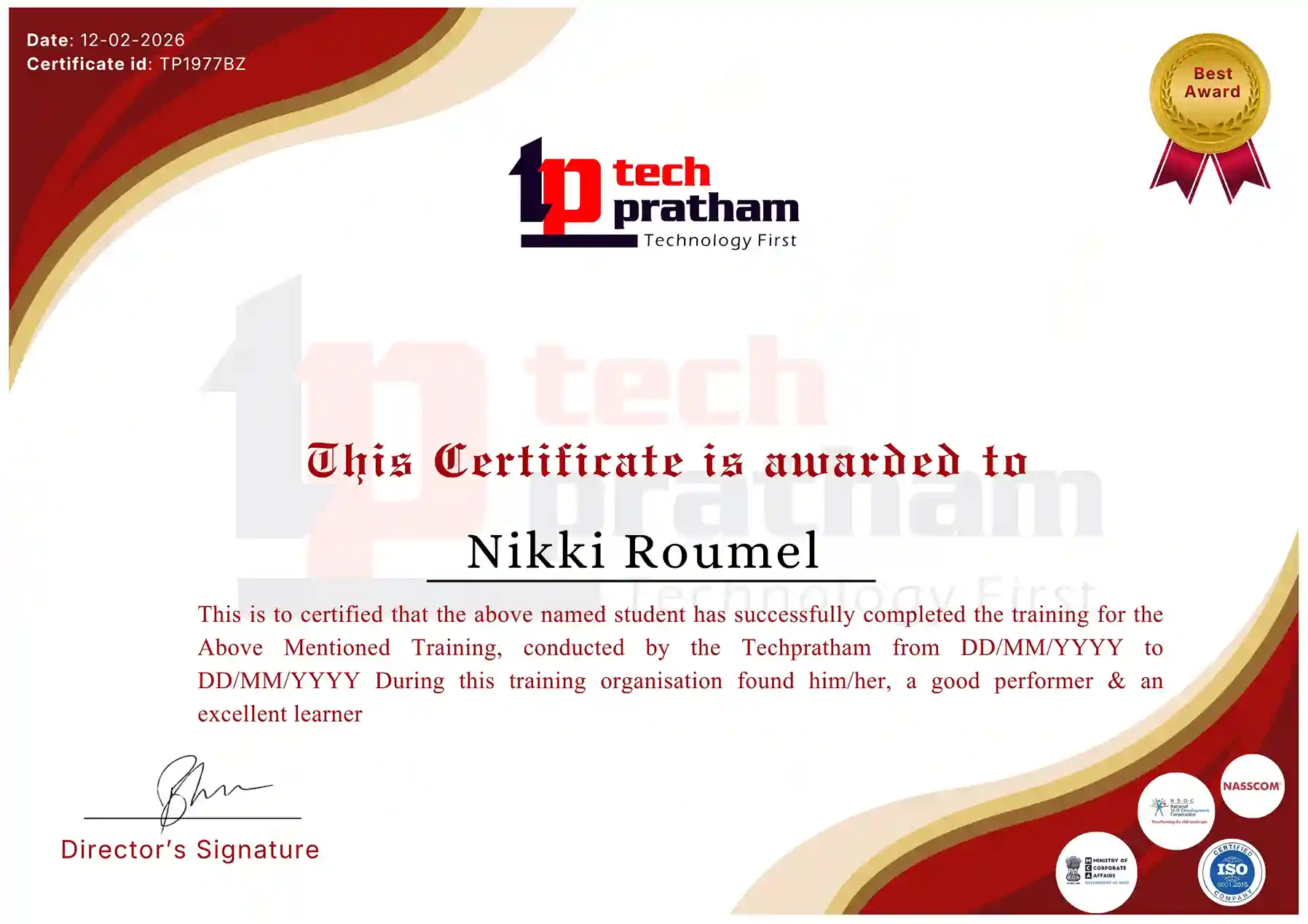
Course Name
News Highlights
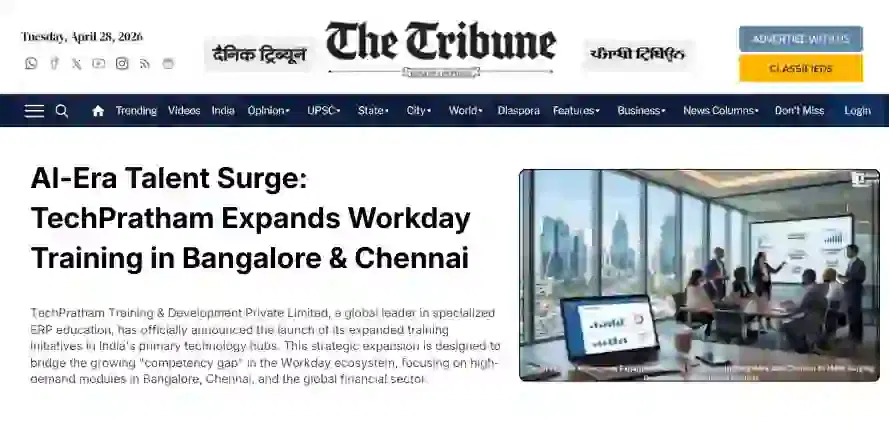
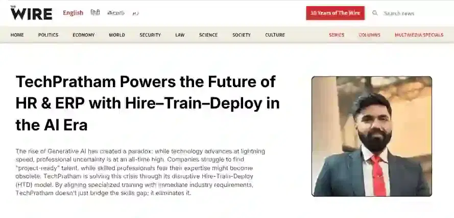
Featured In













About Us
TechPratham is an ISO 9001:2015 certified IT Training and Development, delivering industry-focused certification courses with expert guidance and placement support.
CIN:U62013UP2025PTC223378GST:09AALCT8794N1Z2
Courses
Company
 +91-8882178896
 +1 (343) 477-0926
© 2026 TechPratham. All rights reserved.An ISO 9001:2015 Certified Company